
Schematic, Mask, and Die Shot of Intel’s 4004 CPU from 1971 « Adafruit
Part 1: Computer Architecture Fundamentals (instruction set architectures, caching, pipelines, hyperthreading) Part 2: CPU Design Process (schematics, transistors, logic gates, clocking) Part 3:.
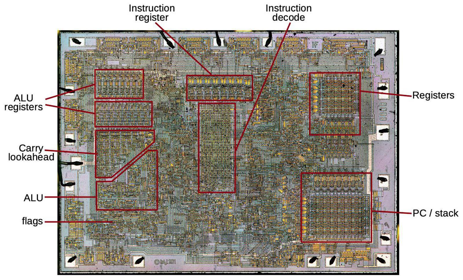
Reverseengineering the carrylookahead circuit in the Intel 8008 processor
Learning Intel's CPU naming schema, at first glance, seems impossible. Compared to AMD, there are a lot more seemingly random numbers stapled onto one another. In reality, though, it's not that bad. Let's start by breaking down one of Intel's most popular and most recent chips, the Intel Core i7-11700F. Intel Core i7-11700F
Review Intel Core i7 and X58 chipset all systems go. FSB not invited
In addition to the 14th-gen announcement, Intel also announced its new Core U Processor Series 1, including the Intel Core 7 processor 150U, which offers up to 5.4 GHz turbo frequency, up to 96 GB.
Review Intel Core i911900K CPU
Intel® Iris® Xe Graphics eligible. Intel® Core™ i7-13700HX Processor. Q1'23. 16. 5.00 GHz. 30 MB Intel® Smart Cache. Intel® UHD Graphics for 13th Gen Intel® Processors. Intel® Core™ i7-13700T Processor. Intel® Core™ Processors product listing with links to detailed product features and specifications.
Micro processor logic gates Electrical Engineering Stack Exchange
Mobile 6th Generation Intel® Core™ Processor Family 5th Generation Intel® Core™ Processor Family Intel® Core™ X-Series Processor Family Desktop 4th Generation Intel® Core™ Processor Family Intel® Core™ processors technical resources list includes applications notes, datasheets, packing information, product briefs, and more.

Intel 4004 Electronic Freaks
Would either of those two software have schematic symbols available for the following pieces: 6th / 7th generation intel core processors PCI-E Memory (DDR3/4 SODIMM) Best Regards, Shawn Tags: schema 0 Kudos Reply All forum topics Previous topic Next topic 10 Replies CarlosAM_INTEL Moderator 07-24-2017 01:13 PM 569 Views Hello, shawn_ahkp:
Schematic circuit diagram of CPU and control unit. Download
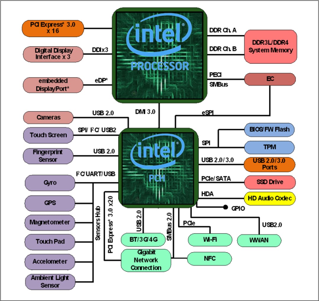
Introduction. This processor is a 64-bit, multi-core processor built on 10-nanometer process technology. The S-Processor Line offered in a 2-Chip Platform that includes the Processor Die in LGA package and Platform Controller Hub (PCH-S). The following table describes the different processor lines:
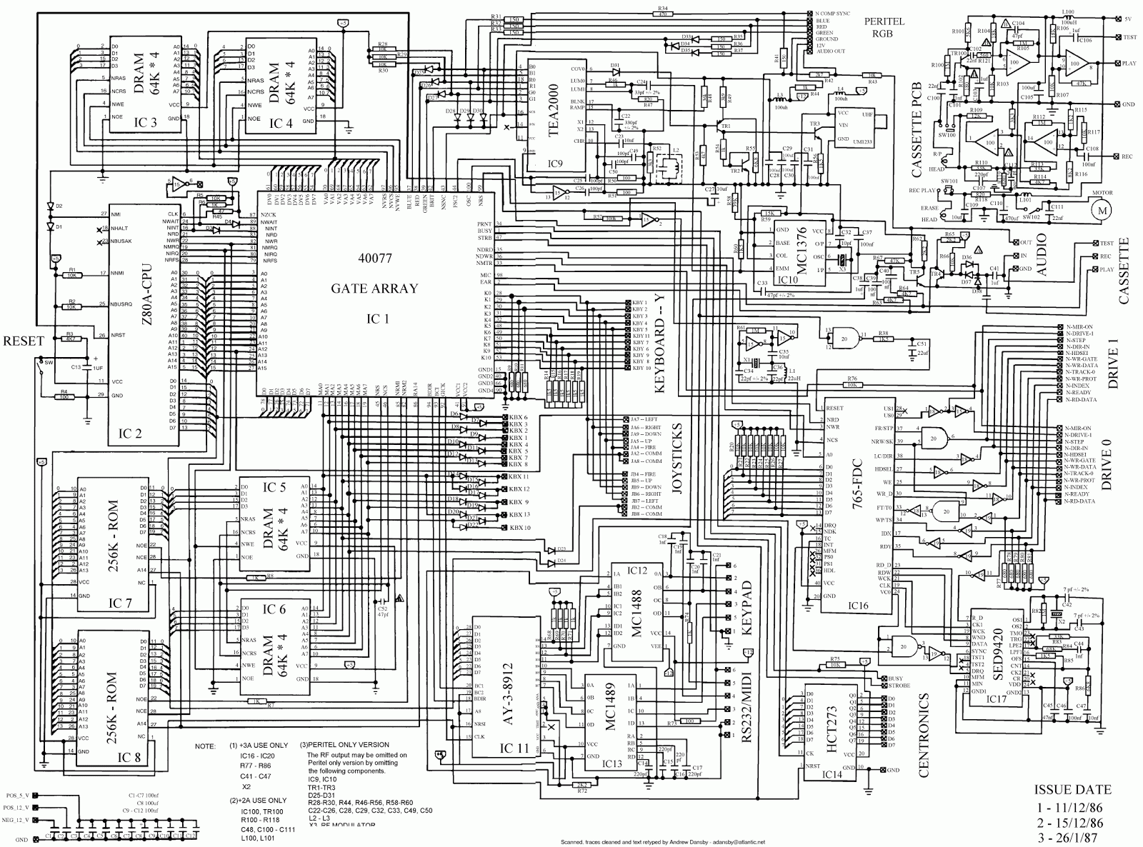
Diagram Of Circuit Board
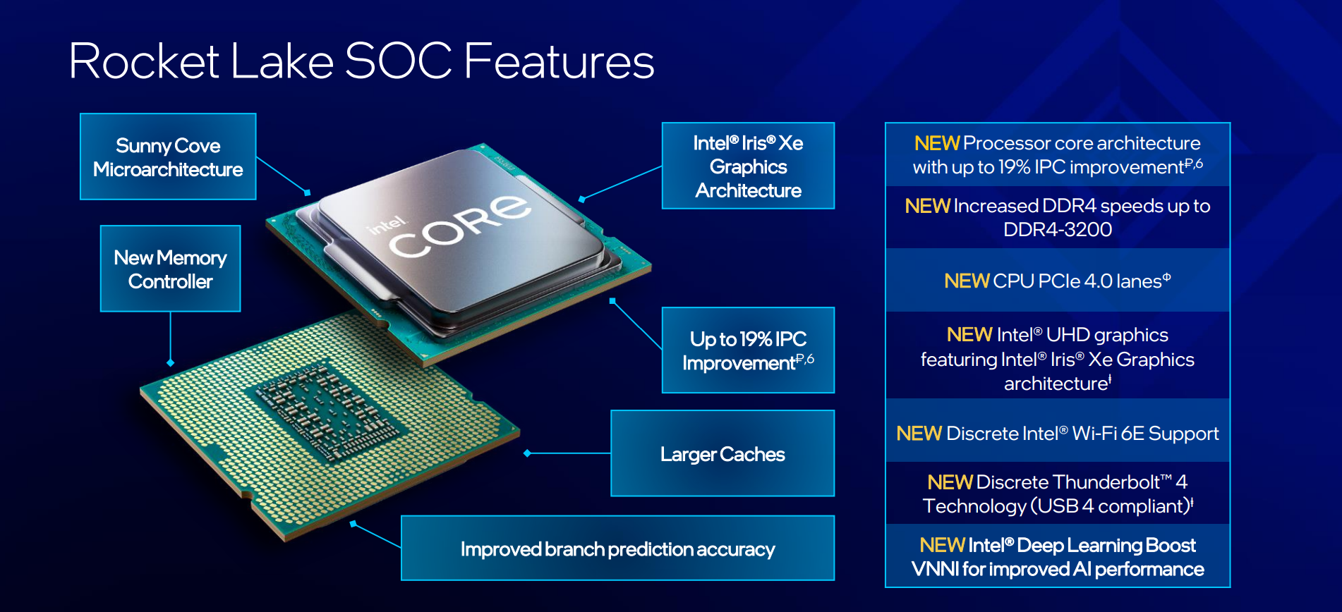
Overview The new Intel® Core™ Ultra processors, Intel® Core™ processors, Intel® Core™ 14th gen processors, and Intel® Core™ N-Series. Updated naming conventions, including the Intel® Processor, the new brand name for our value processors, that will replace Intel Pentium® and Intel Celeron® branding. New processors, new names
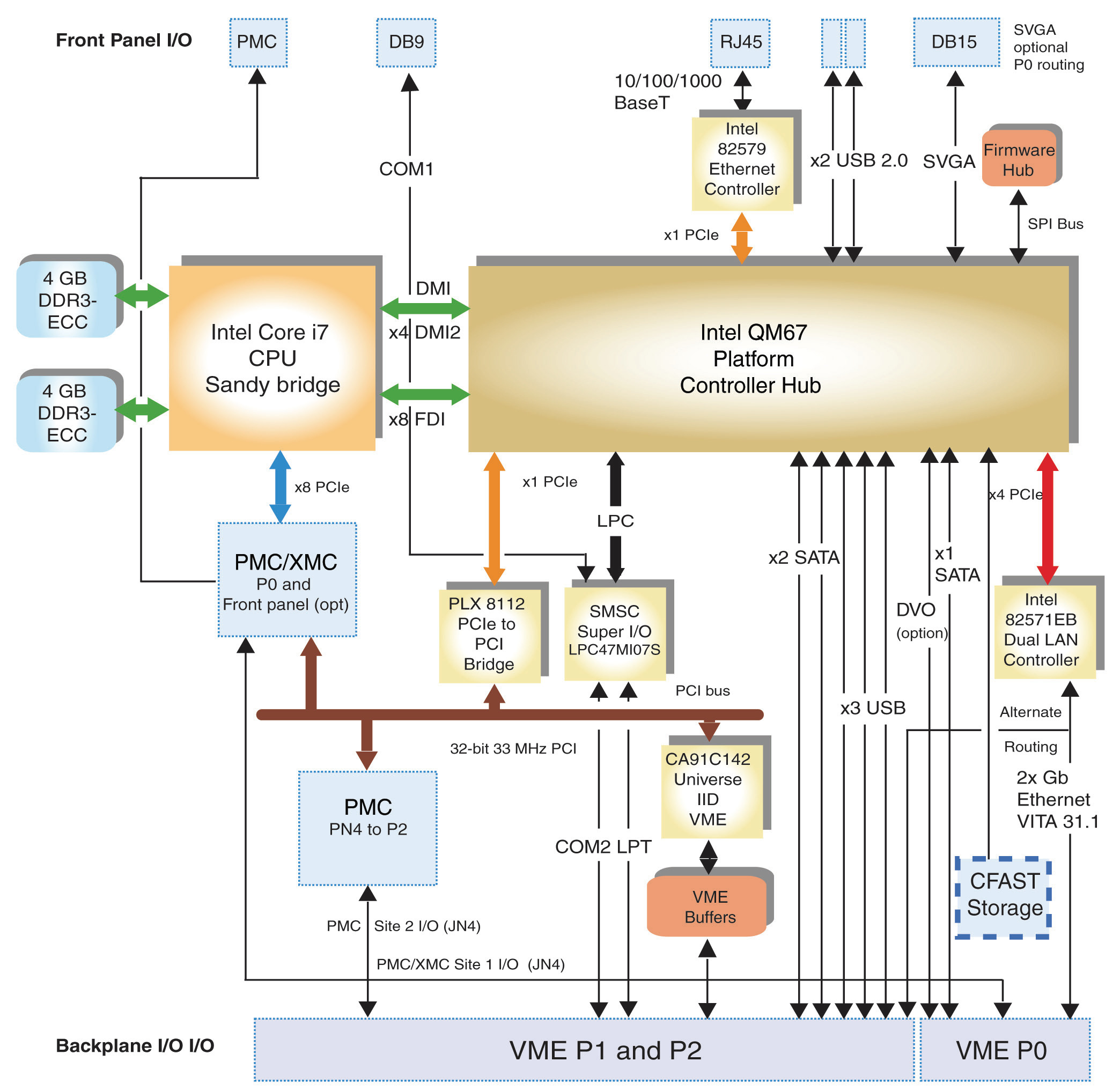
CPU7116 VMEbus SBC Intel Core i7
The schematic diagram will provide a general overview of the circuit, while the wiring diagram will show all of the components and connections in detail. Factors to Consider When creating or modifying an I7 processor circuit diagram, there are several important factors to consider.
Core™ i56500 14nm Desktop Processors Intel Mouser
Launched in November 1971, the Intel® 4004 paved the way for modern microprocessor computing. As the world's first commercially available microprocessor, the Intel 4004 enabled the convergence of the technology superpowers - ubiquitous computing, pervasive connectivity, cloud-to-edge infrastructure and artificial intelligence - and.
Micro processor logic gates Electrical Engineering Stack Exchange
Learn more. This is the third installment in our CPU design series. In Part 1, we covered computer architecture and how a processor works from a high level. The second part took a look at how some.
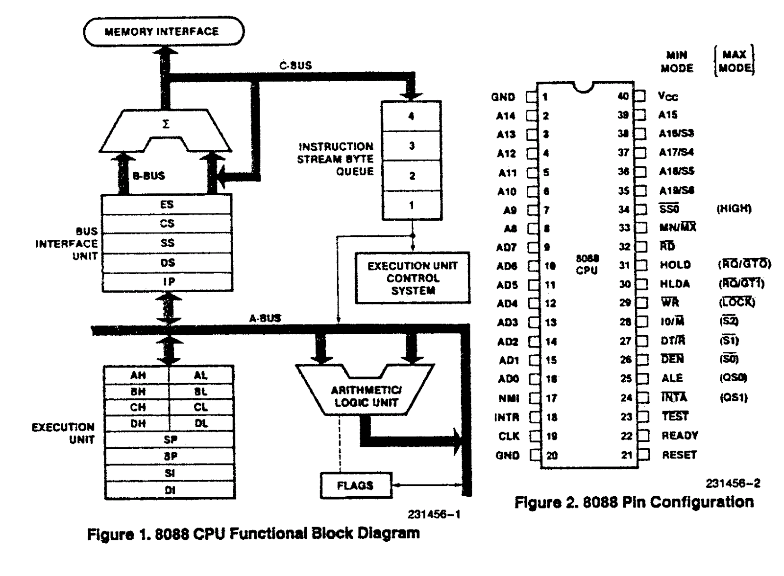
Education for ALL Introduction to 8088 Microprocessor and its Block
Document Number: 337344-006 8th and 9th Generation Intel® Core™ Processor Families and Intel® Xeon® E Processor Families Datasheet, Volume 1 of 2 Supporting 8th Generation Intel® Core™ Processor Families, Intel® Pentium® Processors, Intel® Celeron® Processors for U/H/S Platforms, formerly known as Coffee Lake

Complete Artwork, Schematics, and Simulator for Intel MCS4 (4004 family)
Part 1: Computer Architecture Fundamentals (instruction set architectures, caching, pipelines, hyperthreading) Part 2: CPU Design Process (schematics, transistors, logic gates, clocking) Part 3:.
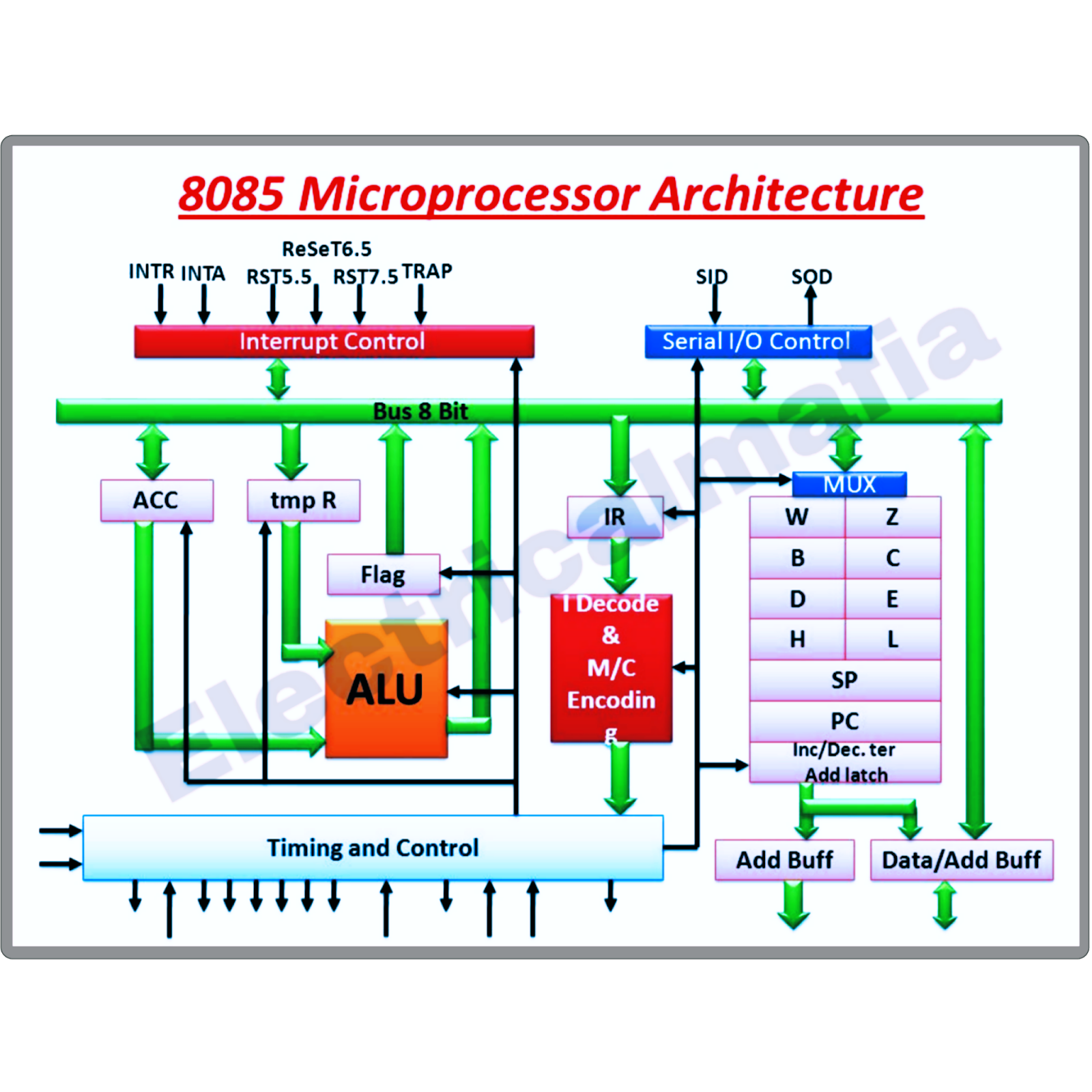
Architecture of 8085 microprocessor ElectricalMafia
1. Design Guidelines for HDMI Intel® FPGA IP x 1.1. HDMI Intel® FPGA IP Design Guidelines 1.2. HDMI Intel® FPGA IP Board Design Tips 1.3. Schematic Diagrams 1.4. Hot-Plug Detect (HPD) 1.5. HDMI Intel® FPGA IP Display Data Channel (DDC) 1.3. Schematic Diagrams Give Feedback 1.3. Schematic Diagrams
Core™ i35010U 14nm Processor Intel Mouser
Intel A80386DX-20 CPU die image. The Intel 386, originally released as 80386 and later renamed i386, is a 32-bit microprocessor introduced in 1985. The first versions had 275,000 transistors and were the central processing unit (CPU) of many workstations and high-end personal computers of the time.. The 20 MHz version operates at 4-5 MIPS.It also performs between 8,000 and 9,000 Dhrystones.

Schematic, Mask, and Die Shot of Intel’s 4004 CPU from 1971 « Adafruit
After completing the verification work for the 4004 microprocessor, I yearned to simulate a complete microcomputer set (CPU, ROMs and RAMs) at the transistor level. In late December of 2008, Tim McNerney sent me scans of the Intel 4002 RAM mask proofs. This was directly usable for the simulator, but the schematics were not available in any form.